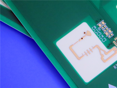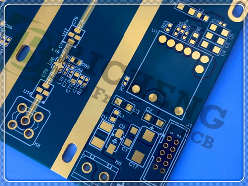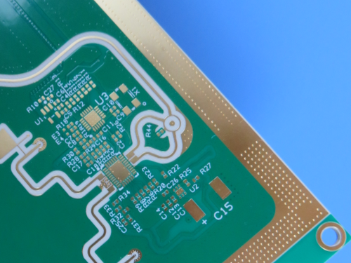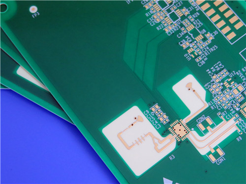
HDI Hybrid PCB 8-Layer 1.5mm RO4003C S1000-2M Advanced Impedance Control for RF and Microwave Circuits1. Introduction to RO4003C Rogers RO4003C materials are proprietary woven glass reinforced hydrocarbon/ceramics that combine the electrical performance of PTFE/woven glass with the manufacturability of epoxy/glass. This design offers superior high-frequency performance and cost-effective circuit fabrication. The result is a low-loss material that can be fabricated using standard epoxy/glass (FR-4) processes at competitive prices. RO4003C materials possess the necessary properties for designers of RF microwave circuits, matching networks, and controlled impedance transmission lines. Its low dielectric loss allows RO4003C to be used in applications where higher operating frequencies limit the use of conventional circuit board laminates. Available in various configurations, RO4003C laminates utilize both 1080 and 1674 glass fabric styles, all meeting the same laminate electrical performance specifications. RO4003C materials are non-brominated and do not have a UL 94 V-0 rating. 2. Features of RO4003C Dielectric Constant: DK 3.38 ± 0.05 at 10GHz 3. Features of S1000-2M Low Z-Axis CTE: 2.4 ppm/°C, excellent through-hole reliability. 4.Basic PCB Specifications
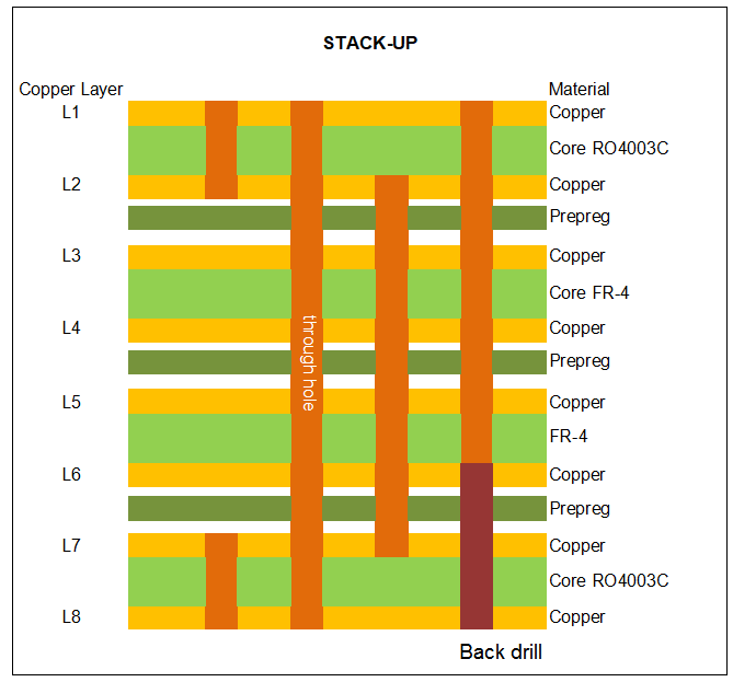
5.PCB Stack-Up (Component Side at Top)
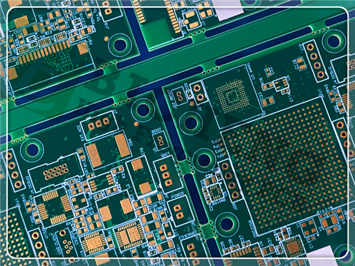
6. PCB Statistics Components: 41 7. Type of Artwork Supplied Gerber RS-274-X 8. Quality Standard IPC-Class-2 9. Availability Worldwide
10. Some Typical Applications Cellular Base Station Antennas and Power Amplifiers |
Get a Quick Quote
Fill in the form below and our engineers will reply within 24 hours with technical specifications and pricing for HDI Hybrid PCB 8-Layer 1.5mm Rogers RO4003C S1000-2M Advanced Impedance Control for RF and Microwave Circuits.